Saturday, November 24, 2012

Voice Recorder with ISD 2590

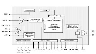
ISD 2590 is an IC recorder and playback sound with a duration of 90 seconds the product from Winbond. To produce sound output, the design of this system is used IC ISD2590. ISD2590 is an IC that can produce sound output based on input entries are recorded into memory IC. ISD25xx is a type of storage IC sound, while xx is the code of the storage duration. Storage duration or length of words that can be stored by the ISD 2590 is 90 seconds. IC 2590 is operated in the address bits means every word is recorded to have its own address. This tool is only a single IC chip, but in it already contains numerous enhancements that help in the operation of sound recording and playback. Additional tools in the form of oscillator, amplifier microphone, Automatic Gain Control (AGC), noise filters, and amplifiers for speakers, so it does not require an additional amplifier to the speakers again. Another advantage of this tool is able to connect with microprossesor and microcontroller devices. ISD 2590 has a special memory for storing voice recordings. Pin connection diagram and block diagram of ISD 2500 is shown in the following picture:


Figure Block Diagram and Pin Connections ISD 2590


The function of each pin is as follows:
1. Input microphone (Mic)
This pin will receive the input signal from the microphone input. Received signal will be amplified by the amplifier (preamplifier) ​​that already exist in the IC. On the Automatic Gain Control (AGC) will be arranged so that the reinforcement that comes out after the preamplifier is-15db to 24 db.
2. Reference microphone input (Mic Ref)
By connecting this pin to VSSA (analog ground) in series with the capacitor, the existing noise on the input signal can be rejected or discarded by the preamplifier.
3. Analog Output (Ana Out)
The advantage of this pin is to provide the preamplifier output to the user. The strengthening of the voltage at the preamplifier is determined by the voltage level at the AGC pin.
4. Analog Input (Ana In)
This pin receives an input signal input to record. On the use of microphone input, analog output pin must be connected to the analog input pin with an additional capacitor.
5. Automatic Gain Control (AGC)
This section is arranged by strengthening the stability of the preamplifier.
6. Speaker output
Differences ISD 2500 series all tools with others that is the speaker driver consisting of an audio amplifier output. output from this pin can be directly connected to the speakers with the power of 16  50 mWatt.
7. Power Down Input (PD)
When not used for recording or playing back, the PD will be logic high, the state is used to generate very little power mode because it is not used. At a low pulse to generate overflow condition, the Pd logic high will make the process of resetting the memory address that points to the starting address. PD pin is used in selection of the operating mode M6 (push-botton).
8. Chip Enable Input (CEI)
To produce active conditions (enable) then this pin must be low so that the condition diberikaan recording and playing back sound to do.
9. Playback / Record Input (P /)
This pin is used to lock (latch) or the state of the currently selected mode. To make a sound play mode, the pin is given logic high. As for the recording process, it is provided on this pin is logic low.
10. End Of Message (EM)
This pin signals when the recording process is completed. Output will issue a credit for the TEOM at the low end of the process output. When the pin is issued a logic low it means the recording process is completed. In the preferred implementation, this pin is usually connected with conditions of low and used to re-ballot player mode only.
11. Oveflow Output (OO)
Low pulse issued when the memory has reached the end of the last space available on the memory, and it indicates that the available memory is exhausted. The output will follow the input pin to reset the PD pulse tools. This pin can be used in conjunction with a series of other ISD 2500 to increase the duration of the recording or playback time in the time you want.
12. Input Voltage (VCCA, VCCD)
Pin it to give input voltage to the IC so that it can work. Limit the input voltage that can be supplied to the IC is 4.5 to 6.5 volts.
13. Ground input (VSSA, VSSD)
        This pin is used to input ground.

Timing diagram of the process of voice recording and playback are shown in the following figure.

a. Process Record (Record)

b. Process Playback Sound

Comparator OP-AMP (Comparator)

In hardware design uses a comparator circuit, which is one implementation of the op-amp function. One characteristic of the comparator circuit is the absence of feedback from output to input. Another feature that is the Vref on one input and ground.

Comparative Picture Association circuit (comparator)
From the figure above it can be seen the following equation:


The working principle of the comparator is the op-amp IC LM 311 will compare the input voltage (VI) with voltage Vref. Vref can be either positive or negative voltages.
If given a positive voltage on Vref, so when the input wave is in the 0 to-Vref or input wave at a negative cycle, then the output voltage (Vo) Vo max will be made achieve positive and at the input waves are in the 0 to + Vref or wave input on the positive cycle, the output voltage Vo will be made reaching negative max.
If the Vref given negative voltage, so when the waves exceed the negative input voltage (-Vref) the output voltage (Vo) will be made higher (up to a maximum voltage positive output voltage. Shown in the picture below wave output responses to input waveform comparison the reference voltage (Vref).


Figure Shape waves in the Comparator Input (a) and form the output:
(b) the positive Vref
(c) the negative Vref

Sensor LM35

In National Analog and Interface Products Data Book (2002) noted that the IC is a precision temperature sensor with a linear output that has a temperature in degrees Celsius rise. LM35 sensors there are two types namely the type and LM35DZ LM35CZ. The difference of the two types that are at the limit of the width of the temperature measurement. The width of the temperature range that can be measured by LM35DZ is 0Celcius to +100 Celsius, while LM35CZ type capable of measuring the temperature with a wider range limit ie-40Celcius to +110 Celsius. LM35 also requires no special calibration to provide accuracy at room temperature about 1/4C and 3/4C less than the width of the temperature range for each type of LM35. LM35 has a low impedance output with a linear output. This sensor uses a single power supply or the plus and minus supply, limits to the voltage source is a-0.2V to +35 V. In application sensor LM35 has an output voltage proportional to Celsius, the output voltage limit of +6 V to-1V for different temperatures according to the width limit of measurement. In addition it also has the LM35 linear voltage output 10 mV / C and low output impedance of 0.1 ohms at a current of 1 mA.

Some type IC LM35

As transistor amplifier Flow


Darlington pair
The advantage of using an amplifier with darlington pair is:
a. Strengthening great.
b. High input impedance but low output impedance.


Figure (a) Basic circuit Darlington Couples


Input resistance:


Description:
hoe = output resistance (Ro)
HFE = reinforcement transistor
r'E = resistance in RE
RE >> r'e r'e to negate the effect, but the RE too large causing the voltage gain will be reduced once.

where:


From Figure (b) may be made following equations:

Resistance input:


Transistor


Understanding Sensor


The sensor is a device that changes of physical quantities into electrical quantities. Temperature is a measure, because it can be measured, monitored and can be used in almost any physical system. The amount that must be represented in an efficient and accurate value to be put to good use. There are basically two ways to represent the value of these quantities, which are digital and analog.

In analog representation, a quantity represented by other comparable magnitude proportional to the amount of the first. The word can be interpreted as an analog line. An example is the mercury thermometer. At the measured temperature change, high mercury in the thermometer capillary tube was also changed following the change in temperature. Characteristics of the analog scale is an important change in the continuous range of values ​​(continuous).

In a digital representation, the magnitude is not represented by other comparable magnitude, but by a symbol called a digit or digits, as opposed to a digital representation of the analog. If the analog value is continuous change, then the change in discrete digital values​​.

Optocoupler or Phototransistor


Optoisolator is a component that is used as a component of the control I / O for equipment that operates with DC or AC voltage. An optocoupler consists of a GaAs LED and NPN phottransistor made ​​of silicon. To use optoisolator circuit can be seen in the image (a) and (b).
In (a) optoisolator get TTL input signal shaped box so that the output signal box, but also in the form of voltage level changed to 0 - +24 volts.

Sensor Optocoupler / Phototransistor

Picture Use Optocoupler / Phototransistor


In figure (b) optoisolator used in the modulated input voltage Vin to Vout isolated peak modulation voltage of +12 V.

Diagram Pin Parallel Port


There are two kinds of parallel port connector, which is 36 pin and 25 pin. 36 pin connector known as Centronics 25 pin connector and is known as DB25. Centronics first and was used from the DB-25 connector. DB-25 was introduced by IBM (along with DB-9, for the serial port), which aims to save space. Since the DB-25 is more practical, to koneksitor parallel port on the computer now only used DB-25.
On the computer, the parallel port connector is installed DB-25 female, thus connecting cable out is DB-25 male. Structure / form DB-25 appear


From 25-pin DB-25 connector, only 17 pins are used for bearer channels and information that serve as ground 8 pin. Seventeen information channel is composed of three parts, namely the 8-bit data; 5 status bits, and 4 bits control. Bit control and status function in the "handshake" in the process of writing data to the parallel port. Here is a table function of pin DB-25 connector.


The circuit Seven Segment CA


In a series of seven segment common anode (CA) to turn each segment is required logic '0 '. Thus a power supply or logic '1 'on the anode seven segment. Typically, the anode seven segment CA granted an additional one particular type PNP transistor as BC 559 or FCS 9012 to set the current flowing in the anode seven segment is not too big. In addition to the anode transistor can also function as a switch on the seven segment CA, because if given the logic '0 'on the base of the transistor then seven segments can be lit in accordance with the logic input abcdefg numbers on seven segment. For a figure that usually use IC decoder 7447 in seven segment common anode and 7448 in seven segment common cathode. So much easier to form the numbers on seven segment using 4 bit data path from 0000 to 1111 to cover all the numbers so the savings pin for data communication. There are also without using a decoder IC but still use the line 7 bits of data on each segment of abcdefg so must make manual configuration of data points.


At seven segment can be made a few digits, eg only 6 digits. So to turn seven segments simultaneously to do the scanning process for each digit seven segment. So the usefulness of transistors on the anode seven segment was very helpful to do the scanning process by switching on each digit in turn along with the turn of the seven data bits in each segment. The scanning process must be done very quickly at all digit seven segment alternately at least 60 times a second to create a seven segment as if lit simultaneously. Therefore to make a multi-digit display on seven segment must have 2 pieces of the data path to the data forming the numbers and data to transfer digits. To save some data lines that combine into 1 piece of 8-bit data path by adding the line demultiplexer and decoder transfer digit seven segment were combined into one 8-bit data path.

Simple application seven segment multi-digit CA to counter.


Transistor


The transistor has two types: Transistor Transistor Bipolar and Unipolar.
Bipolar transistor is a transistor that has two poles junction.
Unipolar transistors are transistors that only have one pole junction.

Bipolar Transistors are electronic components that consist of three legs, the emitter (E), base (B), and collector (C). The transistor itself consists of two types of transistor types NPN and PNP transistor type. Current directions signs on each of the designated type of arrows is an emitter terminal. Components and Symbols transistor, as shown in the image below:

transistor

symbol transistor

Unipolar transistors are FET (Field Effect Transistor), which consists of the N channel JFET, P channel JFET, MOSFET N channel and P channel MOSFET
Unipolar Transistor symbols:

unipolar


Thermocouple


Thermocouple
One temperature sensor which is used for high temperature is thermocouple. The sensor is used for appliances such as hot plates, furnaces and other heating equipment tools. Besides accurate thermocouple sensor is also a sensor that is often used in industry because they have specific standards and good durability. So to use a high temperature in the longer term will be more durable than using a temperature sensor made ​​of semiconductor materials are integrated.

Thermocople Type-K

Hot Plate is one example of a device inside using a thermocouple temperature sensor

VU Meter Led

For fans of electronics, especially audio VU meters are often found on devices such as, equalizer, amplifier, tape recorder, and even an audio mixer. Usually found in the VU meter display that the LED lights arranged in a one color or more. But some are still using a needle as long audio devices. At this time we will discuss how to manufacture VU meter classified as very convenient especially for the novice hobbyist electronics for audio applications. The principle is straightforward and simple preparation that requires only diodes, capacitors, resistors and LED lamps as a viewer. Besides those that add the transistor as a switch or a current amplifier when using a lamp that has a larger power capacity. Here is an example picture VU meter circuit is very simple and easy to make.


In addition to using a diode and capacitor circuit some circuit using IC LM 3915, so it may be simpler to create a series of VU-Meter.


Switching Power Supply


Switching Power Supply
One that we often encounter in electronic equipment these days are switching power supply. In addition to its small, compact and neat, it can also provide benefits that electric currents generated quite large compared to the power supply using a common iron core when considered in terms of the same dimension.

In this switching power supply transformer that is used specifically of using a switching transformer varies in size depending on the size of the strong electric current to be generated. To generate the secondary coil voltage switching tranfo This requires a special circuit in the primary coil, it aims to get the frequency of the AC voltage is very high (typically in the order above 25 KHz) as input to the primary coil switching transformer. Usually the primary circuit switching transformer is special oscillators are commonly used, namely LC oscillator or using a particular IC as osilatornya. Thus the oscillator will be used to control the transistors as switches or FET can also be used to make an input voltage pulse with a current large enough to pass the primary coil transformer switching frequency is of course the same as the frequency osilatornya earlier. One thing that must be noted that for mengasilkan pulse and switching the input voltage to the transformer, the input voltage derived from AC 220 Volt / 50 Hz DC voltage must be rectified first by using a diode and capacitor filter (polar / electrolytes), and if necessary, coupled with the inductor, resistor and capacitor nonpolar great power to adjust the electrical current to be passed to the primary coil transformer switcing. Diodes and capacitors to be used for the rectifier must have values ​​that are tailored to the voltage source that is not easily damaged and are required to view the datasheet for the diode. To use a small current diode IN4007 can be used and if you need larger currents can be used diode IN5408, BY 228, and the like. While on kapsitor filter must use a minimum working voltage of 400 volts DC and note the correct polarity.

Picture diode rectifier for switching power supply circuitBY-228 type

Understanding Of Microcontroller

In the world of electronics, microcontroller very important role in the advancement of technology. Moreover, to reach out to many sectors and fields ranging from teaching interests, until it can be applied in their daily lives, even can also be used in larger scale ie in the industrial world. Maybe that makes microcontroller is superior to other control device that is besides the price is relatively cheap and easy to reach because there are a lot of electronics in stores. microcontroller is a lot of choice and variety, ranging in size flash memory used to store programs, and support features such as complete microcontroller ADC, timers, counters, PWM, serial communications, I2C, SPI, and others. This microcontroller also widely produced some companies such as Atmel, Microchip, and others. So that we can choose according to their needs that we need.

understanding of microcontroller

Atmel microcontroller Studio 6 for the latest version


Atmel microcontroller Studio 6 for the latest version
Has released software for Atmel Studio 6 in May 2012 that more comprehensive than the previous version and includes more recent version of the microcontroller and a few additional features. Atmel AVR Studio 6 has support for all types of 8-bit AVR microcontrollers and 32-bit, as well as microcontroller SAM3 and SAM4. The software has also added some special functions and update the previous features that exist in AVR Studio 5 and AVR Studio 4. For more details can be read in a brochure or Atmel Studio 6 can also directly visit the Atmel website.
  New Display Peoject Atmel Studio 6

Atmel Studio 6
Device selection menu selector


Form worksheet creation software


Few Problems On Downloader USB AVR AVR mk II for codevision


Few Problems On Downloader USB AVR AVR mk II for codevision
When our laptop users who have a hobby of tinkering with microcontrollers we might prefer something more devices easy and convenient to fill in the program that we have made to the minimum system microcontroller AVR. So the USB downloader is a very precise and piihan probably already widely available on the market today.


But there sekikit problems arise later on, especially if we are already accustomed to playing microcontroller using C language that is the AVR CodeVision Versions 2.05 or below. Maybe if already accustomed to using assembly language or the AVR-GCC on the AVR Studio it will not be a problem.

If we buy a USB downloder that have been circulating on the market today that we will probably get is a downloader USB AVR AVRISP Mk II version is no longer STK 500 as the previous version. Obviously this will make a bit of a problem in AVR CodeVision users who need a device or a USB downloader. Because the USB downloader Mk II turns out to require a driver to be picked out of AVR Studio is by installing AVR Studio first. As we know now Atmel has been issued for the software that is up to version mikrokontrolernya Atmel Studio 6 which update previous versions AVR Studio 5. If I had previously used frequently using AVR USB downloader version 500 for CodeVision AVR STK no need to install AVR Studio since drivers already available alone.

It makes the problem when we want to fill in our program that have been created using AVR CodeVision and we took the drivers by installing the Atmel AVR Studio 5 or Studio 6. The problem that arises is when the charging program or flash microcontroller program to be "error", or even no response at the time of the flash program to the microcontroller. Yet when checked the settings on CodeVision AVR programmer Mk II driver already exists and is in the set, while in the "device manager" in the windows and installed also appeared normal. But when we try to re-flash program error still appears when we use codevision AVR, but when we try to use Atmel AVR Studio 5 or Studio 6 is no problem and perfectly normal.

After dizziness tried many times using AVR CodeVision might not ultimately be tried again check the settings and select the USB programmer Mk II there was a warning that turned out to require CodeVision AVR AVR Studio version 4:18 or earlier. Then I try to install AVR Studio version 4:19 because that which I still have on my laptop even though there Atmel Studio 6. After that I tried again using AVR CodeVision and tested in flash mode and it worked and success. Means I get to the conclusion that if we use CodeVision AVR and downloader software that we use is USB USB AVRISP Mk II, then we must first install AVR Studio version 4:19 or earlier to replenish the program or programs to flash AVR microcontroller via USB even on computers or laptop may be available or the Atmel AVR Studio 5 Studio 6.

Hopefully useful.

How to Calibrate Oscilloscope


Oscilloscope is typically used for counting the frequency or magnitude of the voltage (amplitude) of a wave or electrical signal. Most people will use an oscilloscope to observe the shape of a sinusoidal waveform of the circuit or power source of alternating current or AC (Alternating Current) so that counting can directly magnitude below the peak amplitude of the wave to the top of the top, so it is often known as the peak to peak voltage (Vpp). But to do the calculations and get an accurate result it must be ascertained in advance that we will use the oscilloscope has been calibrated or not. To determine if the oscilloscope has been calibrated or how to calibrate I will explain as follows.

Oscilloscope basically there are a few main buttons that have different basic functions, among others.
Volt / div is used to set the voltage measurement or amplitudo in 1 box or div to limit the position of the top and bottom of the box. More precisely to determine the magnitude of the voltage which is calculated in each box.
Time / div is used to determine the limit of the measurement period (in seconds) or limit the left side and right side in one box or div.
Mode is to determine which channel is active or appear in the display. Generally can be one channel or both channels simultaneously, even to combine both the channel.
var on the volt / div is used to calibrate the voltage on each channel on the oscilloscope. The effect on the settings button that changes the distance up and down on one wave.
var on time / div is used to calibrate the period on all channel oscilloscope. Securities that comes up on the settings button that changes the distance left and right on the first wave.
Position on y to adjust and shift the location of the top and bottom of the wave on the screen.
Position on x to adjust and shift the location of the left and right waves on the screen.
For more details please look at all the buttons on the oscilloscope picture below .

Oscilloscope

The main image on the oscilloscope.

After all the functions of the buttons on the oscilloscope are understood then we can begin to do the calibration. First, we turn first osiloskopnya. Ensure that there is a line drawing on the screen and it was clear and not blurry. Where do they blur the focus setting prior to turning the focus knob below the screen, and check whether the line that looks slanted or straight? If a line appears slightly tilted immediately fixed by turning the settings on the slope of the hole in the bottom of the screen by using a screwdriver (-) small. After all the initial setup has been completed, immediately prepare an oscilloscope probe to be used. Since the function of the oscilloscope probe is very important to connect each channel oscilloscope on the device which we will measure and can be used to calibrate the oscilloscope itself. Oscilloscope probe itself is in addition to functioning as a link can also be used as a factor when the sources nor will we measure the circuit has a voltage oscilloscope than the maximum capacity, because there is a switch on the oscilloscope probes were labeled X1 and X10. The switch is usually only found on the original oscilloscope probe so by putting the X10 position we can still measure the voltage source greater than the measuring oscilloscope (volts / div) to 10-fold the maximum limits of the oscilloscope. But for homemade oscilloscope probe we can only use a maximum limit 1X on the oscilloscope.

Picture Probe oscilloscopes
In the picture above looks a switch on the original probe, but make sure the position of the probe remains on the X1. If the probe does not have the original can be used homemade probe using a good quality cable and alligator capi. Put the probe on channel 1 and select the mode switch on channel 1 (CH1.) as shown in the picture below.

Determining the mode on channel 1
After installing the probe on channel 1, position the probe tip at Cal existing terminal on the lower left corner on the oscilloscope screen. Note the inscription on it says that cal terminal 2 Vpp and 1kHz. That means the oscilloscope should be calibrated so that the value of the peak to peak or peaks up and down on the div box worth 2 volts and a frequency of 1 KHz 1div. In the picture below is a picture of the waveform calibration has not been done as yet to meet the existing rules on the terminal posts cal.

Placing the oscilloscope probe to the terminal cal.
The second step should be done for calibration is made ​​so that the values ​​calculated in the first box is 2 volts. The limitation used in the volt / div important free calculation results is div 1 box or 2 Volt. Rotate button var near the volts / div to adjust or calibrate the voltage on channel 1. When the value of one box is exactly 2 volts as shown below means calibrating the voltage on channel 1 has been successful. Then proceed to do kalibrsi frequency. Figure panels on the oscilloscope

Waveforms are in calibration voltage.
To perform the calibration voltage waves make the value 1 (one peak and one valley) on the square wave is 1 KHz. The way is set the volt / div square wave pulse that is easily seen (try the value of 0.5 ms or 1 ms only), and then turn the var below or near the time / div (var remember the time / div ...!). For example I use the time / div to 0.5 ms then I had to get the waveform peaks 1 box 1 box 1 box and 1 valley. So later when calculated value of the wave period of 1 (one peak and one valley) is 0.5 ms + 0.5 ms = 1 ms (the value of the wave period). Then the frequency f is 1 / T = 1/1 ms = 1 / 0.001 = 1000 Hz = 1 KHz (corresponding to a value of 1 KHz at Cal terminal right ...?). For more details, please see the picture below. Keep in mind that the value of var on the calibration of the voltage on channel 1 was already done, so do not ever change at all, if you do not have to repeat the calibration voltage channel 1 from the beginning again.

Setting time / div for frequency calibration
Waveform after calibration voltage and frequency
After doing all the above steps means the oscilloscope on channel 1 is calibrated voltage and frequency, it is ready for use. But channel 2 also requires calibration, so if we will use the oscilloscope channel 1 and channel 2 2 then the calibration should be done, but remember enough to calibrate only the voltage (volts / div), no need to get to the frequency (time / div) because for frequency calibration effect on channels 1 and 2. To test whether the calibration results we've succeeded or not to use an output voltage of the transformer, eg 12 volts AC with a frequency of 50Hz PLN.

Testing oscilloscope with an AC voltage source
In the picture above, we see that the wave that appears on the screen wider than the screen, change the volt / div at 5 volts.

Waveform sine amplitude limit
After setting on the volt / div then the form of a sine wave can be seen clearly on the oscilloscope screen as below.

Waveform after setting the limit amplitude (volts / div).
To further facilitate the calculation of voltage and frequency at the same time then set the time / div so the sine waveform will be obvious and easy to calculate the amplitude and period in the first wave.

Waveform after adjustment period (time / div)
After drawing pins can be calculated magnitude of the amplitude and period. Firstly may we count Vpp amplitude which is the value of the wave. The amount measured was 3.4 box (3 box + 2 strip line inside the box, each strip 0.2) and the volt / div that I use is 5 volts / div, then the value of Vpp is the sine wave is 3.4 div x 5 volt / div = 17 volts. So the magnitude is 17 volts Vpp, Vrms for her stay divided only by root Vpp Vpp multiplied 2 or 0.707. It will get Vrms = 17 x 0.707 = 12.019 volts (according to the inscription transformer). Furthermore, would we count what is the frequency? It may make it easier to position the top and bottom can be arranged in advance so that the wave is easy to obtain midpoint as shown below.

Adjustment of the position to calculate the period of a wave

For counting frequency then we need to know in advance the wave period. Based on the picture above it appears that the period (end nodes left and right) are 10 div x 2 ms / div = 20 ms. So the frequency is 1 / T = 1/20 ms = 1/0, 02 s = 50 Hz. Means of measurements using an oscilloscope on the output transformer 12 volts is 12.019 volts AC with a frequency of 50 Hz.

Hopefully above is useful as a baseline early, especially those wanting to learn more about Lissajous oscilloscope to find a model, compute the op-amp gain, integrator and differentiator.

Keep in mind that some models of the oscilloscope to the location of the button may vary slightly, but all the functions are the same as described above.